The µLevel is one of my pet projects that I started after needing a bed levelling feature on my 3D printer. I had built a Hypercube 3D printer that I never really got working properly. So I ended up selling it and bought a Creality Ender 3 instead. This means that the project has been put on hold since it was designed pretty specifically to the Hypercube. However I might pick it up again. Never the less you can read more about it below.
The basic idea was to use the cheap PCB manufacturing options in China such as JLC, to create a strain gauge. This would then sit on top of the 3D printer nozzle. When the nozzle touched the print bed during levelling, it would then alter the resistance in the strain gauge, causing the following circuitry to trigger. The advantage of this over, say a standard touch probe would be that everyting was moved away from the nozzle. Really it was part of a bigger plan I had to try doing some real 3D printing.
All standard FDM printers today are actually only printing in 2.5D. Think about it. The printer is doing one layer at a time and does not change its Z-axis while printing any one layer (other than accomodating for differences in platform heights). So to do some real 3D printing, we need to have the nozzle moving in the Z-direction actively while printing. Teaching Tech did a Youtube video about it which peaked my interest.
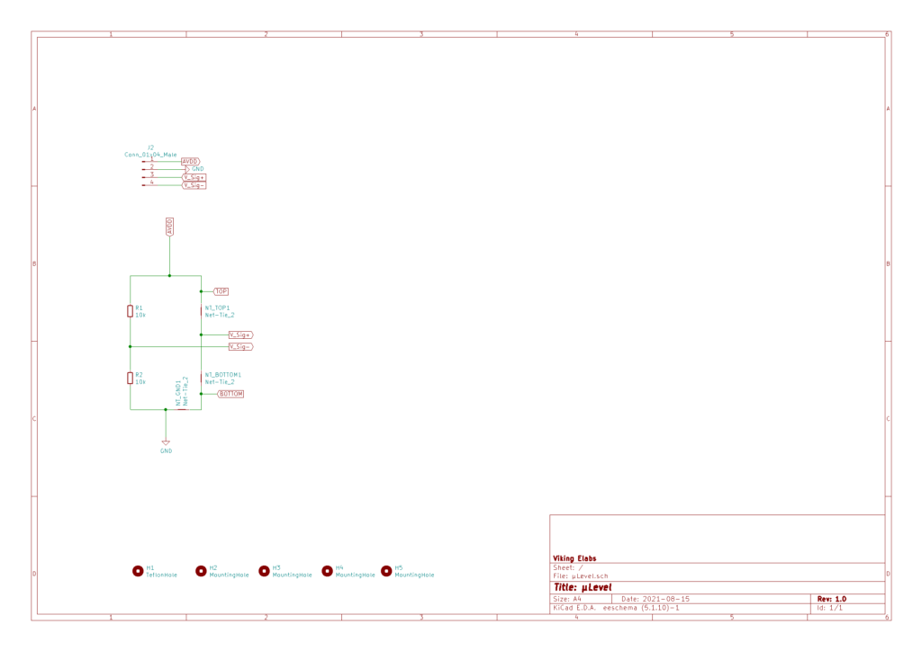
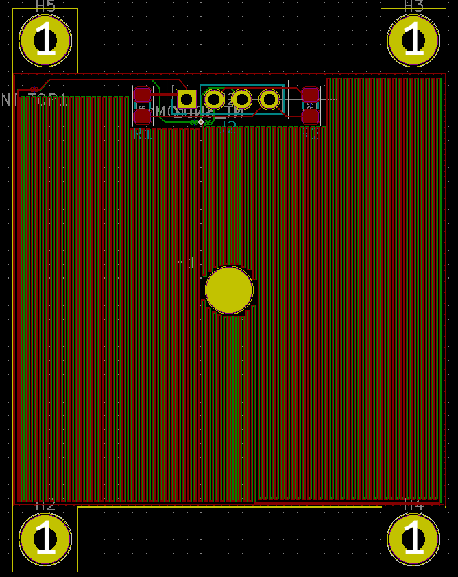
Anyway, I digress. The µLevel removed one of the things in the way of doing this type of printing. I designed a small board in KiCad that utilizes the Wheatstone Bridge. Basically it is a half bridge. The PCB is 2-layers and there are 0.127 mm traces that fills out the majority of the top and bottom layers. On the top layer there are headers and two resistors acting as the other half of the bridge. The traces on either side are each a resistor.
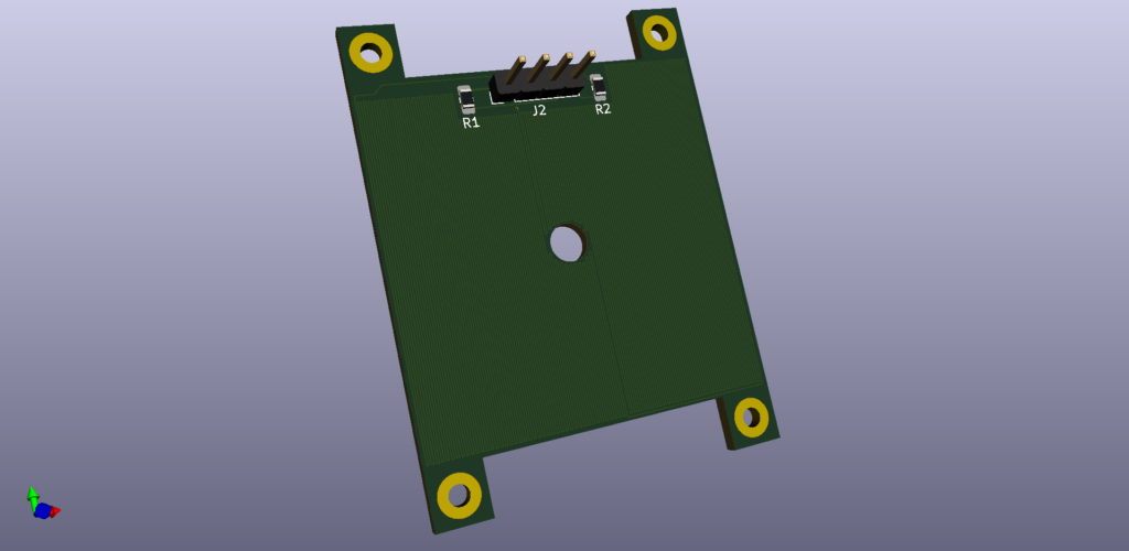
The trace resistance of the top and bottom layer are each around 22 ohms. The reading is taken between the two, basically making them a voltage divider. The trace resistors are sitting on parallel to the two SMD 10k ohm resistors, creating the bridge. The schematic is shown below, very rudimentary.
PCB design is shown below
A wheatstone bridge works by a difference in voltage between the two probing points. Voltage differences between V_Sig+ and V_Sig- shows whether the PCB is strained or not. There should be no difference between the two voltages if there are no strain on the PCB if the resistors are 100% matched. In practice though, there will always be a small difference since there are tolerances in the traces and in the SMD resistors. This can be accomodated for in software and hardware.
The voltage differences are tiny even when straining the gauge. Hence amplification is needed. I used an AD620AN instrumentation amplifier, which adds very little noise to the signal. The AD620AN has a very simple gain selection as it is resistor programmed. Whatever resistance is seen between pin 1 and pin 8 corresponds to a gain. I tried several different configurations, but found 249 ohm (199.4x gain) worked alright.
Initial results where quite promising when testing on the bench. I could hook up a scope to the output of the amplifier circuit and press down on the PCB. I would see a decent amount of movement in the voltage. When I hooked the output up to an ADC on an Arduino, I could also see a good amount of change in the output. However I was worried that I had to press too hard on the PCB compared to having the nozzle press.
I created a new nozzle mount for the printer and mounted the PCB on top of it. I then started moving the nozzle toward the print bed. It would trigger but it needed way to much pressure. So much that the aluminum platform mount started twisting.
This is around the time where I sold the Hypercube and bought a new printer and the project has been on hold ever since.
Though I do have some ideas on how to improve it. I recently noticed that PCBWay will do thinner PCB’s. The current protoype is built with a 1.6mm FR4 print from JLC. However PCBWay will do a 0.8 mm FR4 board for the same price. Of course the ticker the board, the more force it takes to bend it. Standard strain gauges are printed on something that look like a flex PCB so it takes as little force as possible to bend it.
Update 1
I got the board manufactured with a smaller thickness and that did feel a lot better. They were way easier to bend a showed a lot of voltage difference in the oscilloscope. Shortly after they arrived, an assistant professor at OHSU contacted me because he was interested in seeing of the boards could be used for one of his projects. I shipped him all of them, but unfortunately, I have never gotten any feedback. So I suppose they were no success.
The project is open source and KiCad files can be found on my github.