For a few years I have been intrigued by the badge life industry and the PCB artwork enthusiasts. I’ve always wanted to do my own PCB artwork but I didn’t just want to do it on any old PCB. By that I mean, I didn’t wanna take one of my practical designs and make an artwork out of the traces, silkscreen etc. I wanted to make a PCB entirely as the artwork.
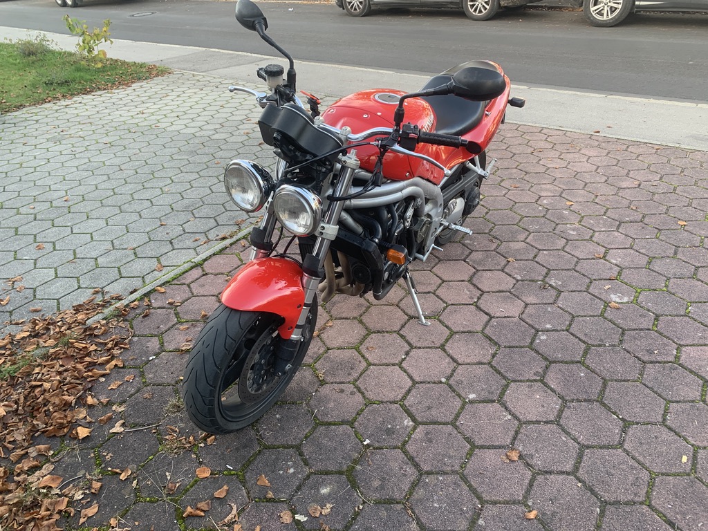
Picture of my Triumph T509 Speed Triple
When I moved to Germany I got myself a new motorcycle. A Triumph T509 Speed Triple. Oh how this is just a great bike! And the iconic just looks just has me sold everytime I see it. The twin round headlights just completely makes the bike. So I thought it might be cool to have a keychain for the key to my new bike. I decided to find a high quality photo of the bike online, and then trace it with the details I wanted. Granted, a keychain has to be fairly small. So it became clear to me as I was tracing the bike in Inkscape that I could not get every little detail. Which is also just an artform in and of itself. Whenever an artist is simplifying something, I feel like it comes very intuitively to them what details they should include in order to make it resemble the original, but in an elegant way. Well… I do not posses these skills as of yet. Maybe one day. Anyway, the plan was to sketch out the motorcycle in Inkscape and create a kind of oval keychain. Tracing takes a long time, that’s for sure. But it’s kind of meditative and you really have to focus to get it the way you want. I actually started out by doing the tracing on my iPad, but when I transferred it to my computer, I realized that i couldn’t change the width of the lines I had traced. Which is kind of important because I wanted the lines to become the copper traces on the PCB. The resulting Inkscape project looks like this
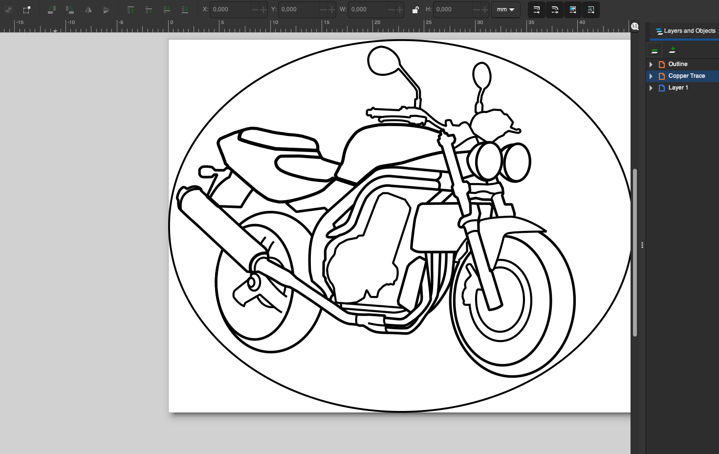
Inkscape vector drawing for export to KiCAD
One very important thing to think about when in the Inkscape stage is the size of the project. Like a keychain shouldn’t be very big. I wanted something that was about 4 cm across and whatever that then corresponded to in height. So I scaled the oval to be 4 cm across. The traces where scaled according to the design rules of the PCB manufacturer. I’ve used AISLER for this project, so if you use someone else, you may have different design rules. So the minimum trace size I could use was 0.2 mm. Which somewhat limits the amount of details you can include since the PCB will be so small.
Next step was to transfer the layers individually to KiCAD in order to create the actual PCB. I exported the oval outline to an SVG file. Then in a PCBNew project in KiCAD, there’s an import optoin to import a graphic, which we can put on the edge cuts layer. Which means that we now have specified the borders of the PCB.
Now we can start importing the details. In this case, I have only worked with the idea of making the copper traces visible and using them for the sketched motorcycle. In order to expose the copper, we need to let the production house somehow know that they should put no soldermask on that part of the board. We can do this by creating a new footprint. Then we use the build in image converter in KiCAD to convert a PNG of the traced motorcycle to something KiCAD can work with.
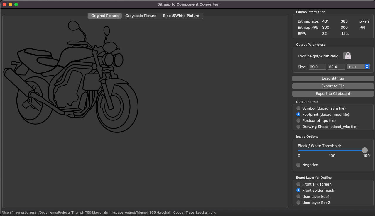
KiCAD image converter tool
When you have done this, you choose copy to clipboard.
Then a new footprint needs to be created in the footprint editor. I usually just make a project library, because these types of footprints are usually only needed for one project. Paste the result from the image converter into the newly created footprint editor window. Choose to edit the footprint and select either the front copper or back copper layer. In order to remove the solder mask over these traces, we actually need to paste the result from the image converter into the footprint editor again. Then align it such that the newly pasted footprint is sitting right in top of the one you put on one of the copper layers. Then choose to edit it and put it on the corresponding mask layer.
{% include figure.html path=“assets/img/projects/triumph_keychain/footprint.png” class=“img-fluid rounded z-depth-1” zoomable=true %}
And that’s basically it for this project. Now it is possible to use the footprint in the PCBNew project. So it is just a question of aligning it. So this is the resulting PCB design
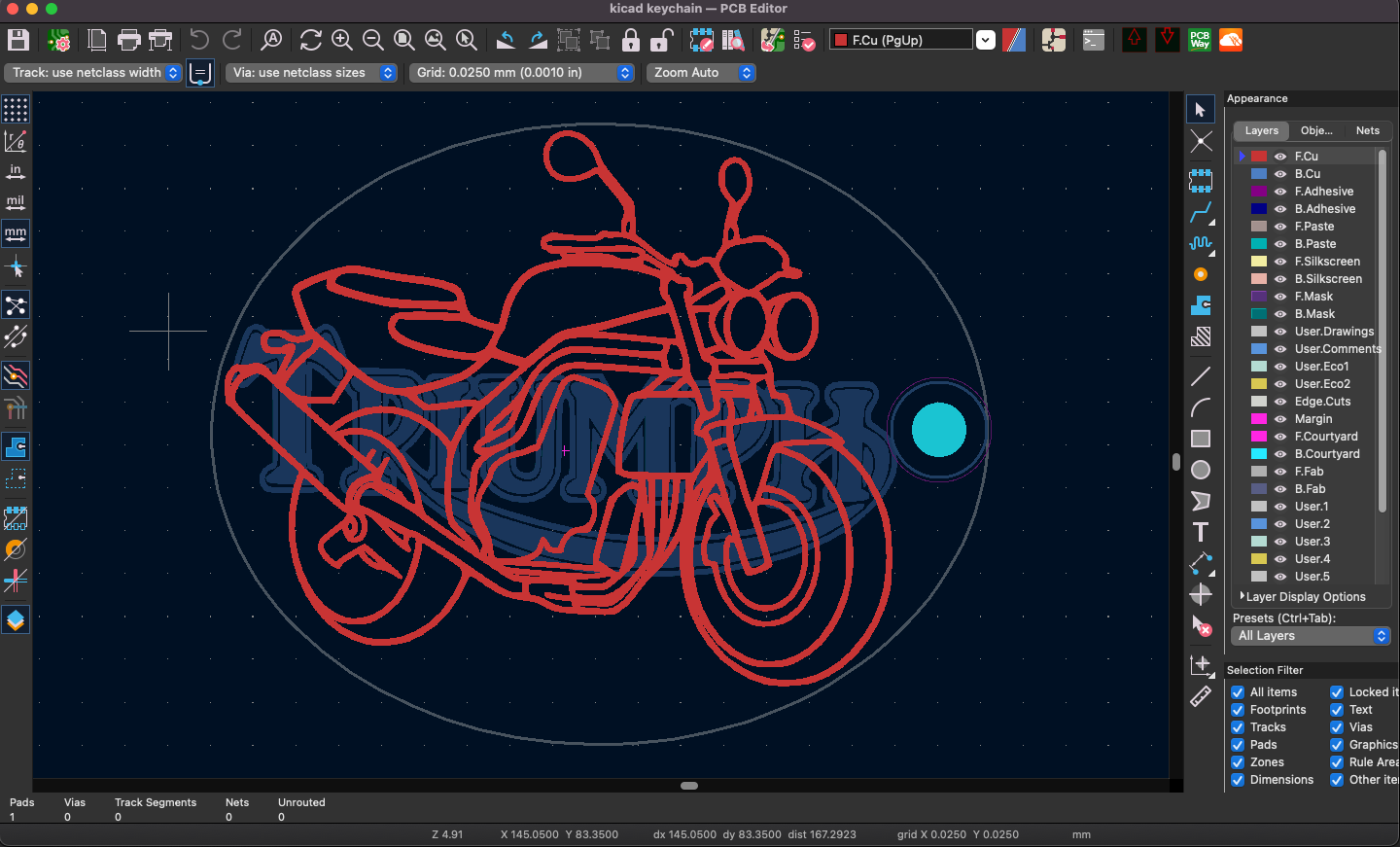
KiCAD PCBNew view of the board design
For this design I really wanted to use a black solder mask. But I knew I also wanted to traces to be ENIG, i.e. an immersion gold finish of the traces. Otherwise the traces would be silver which I didn’t think would look as nice. Only problem is that while most chinese low cost manufacturers will do a black board without any surcharges, they will not do ENIG cheaply. Like PCBWay wanted about 40 USD to do the ENIG finish. Meanwhile AISLER, who are in Europe, will only do green PCB’s. But they will do an ENIG finish for almost no money. So I chose to go with them. They also have a plugin to KiCAD which makes it possible to upload the design to their website with only one click. The results are below
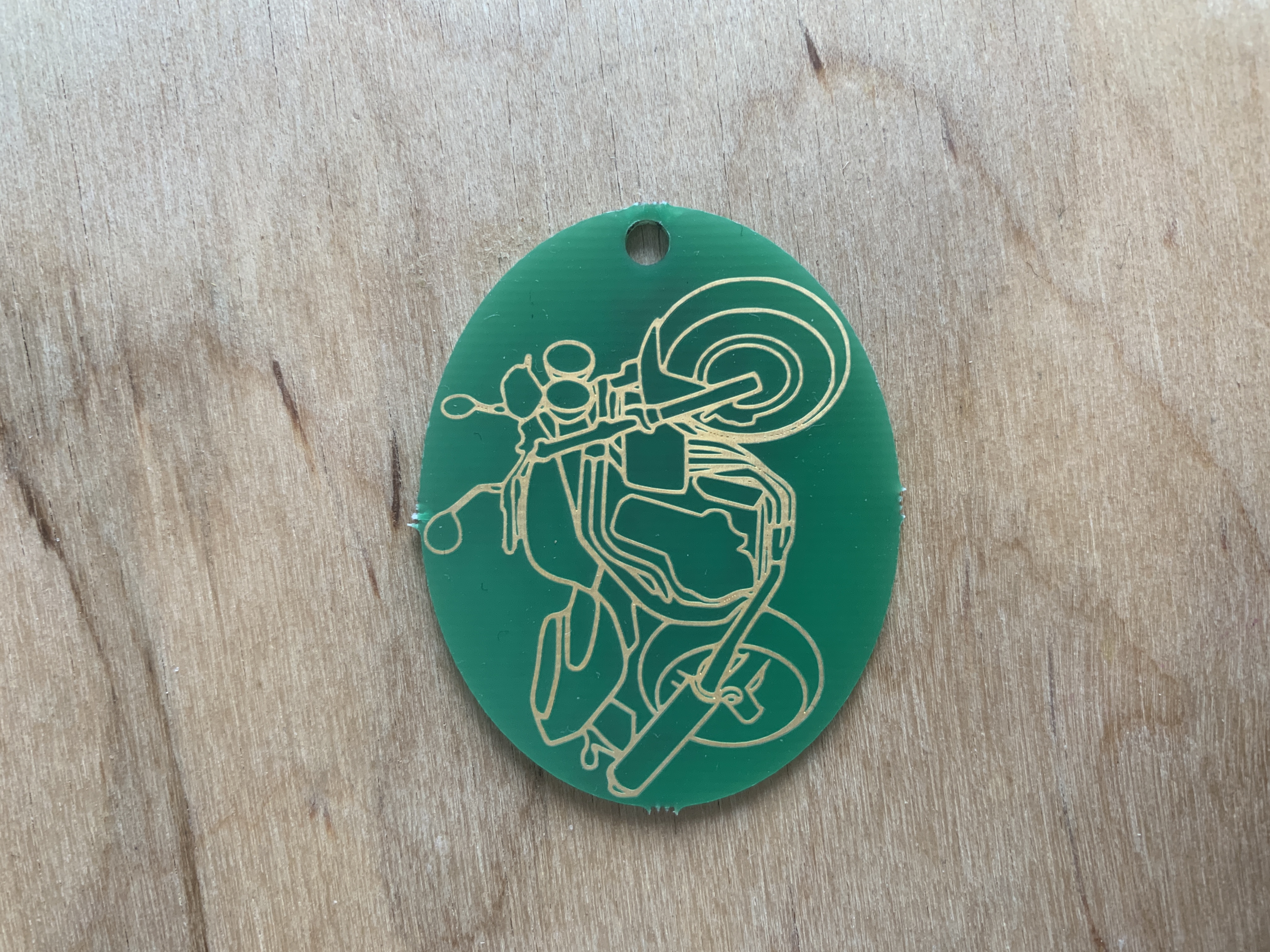
Front side of manufactured PCB
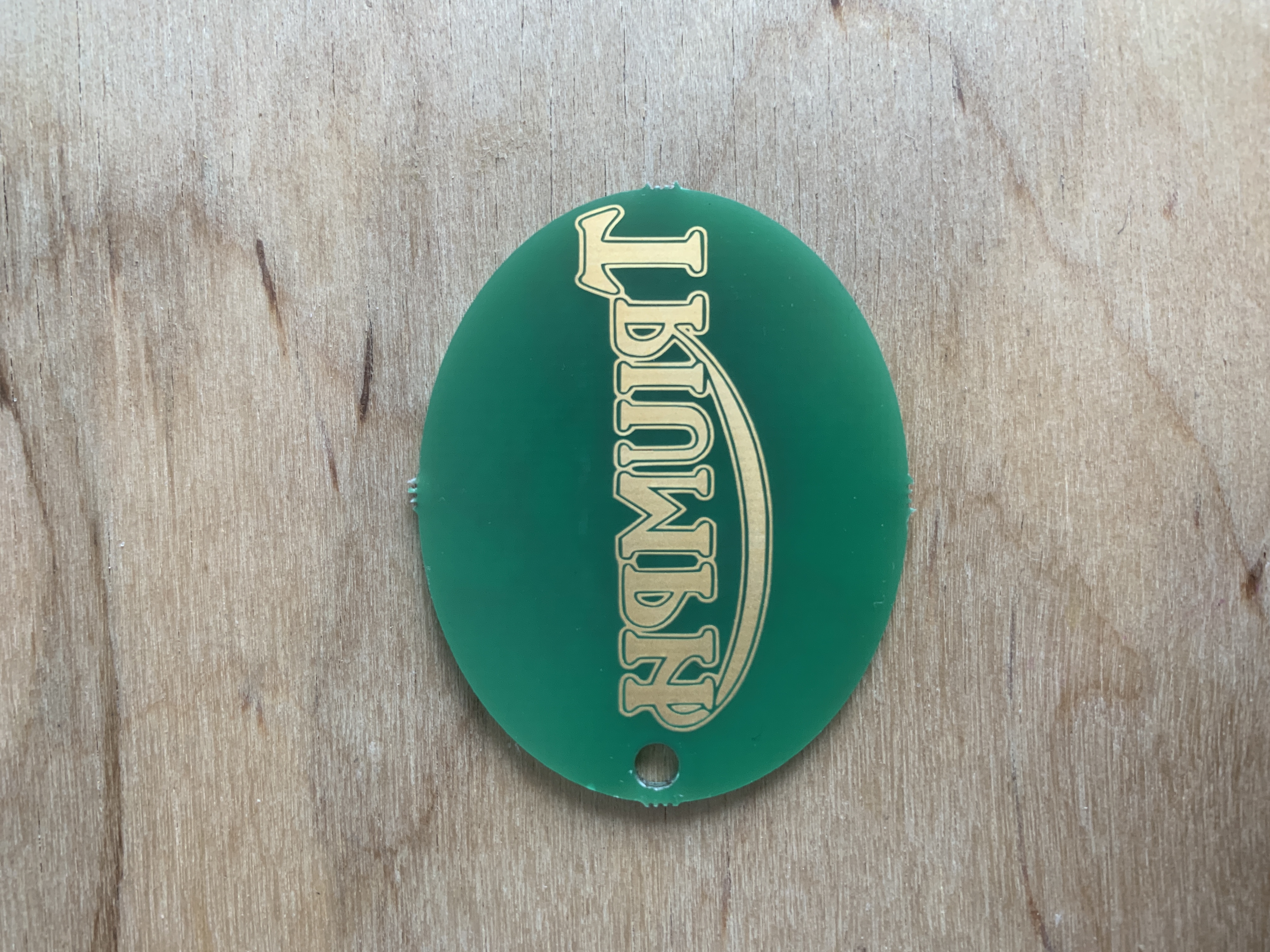
Back side of manufactured PCB
In my own opinion I think they turned out better that I could have ever imagined. I’m so pleased with them and what a great end to a first PCB artwork project. Only issue was that I flipped the Triumph logo the wrong way on the backside, whoops. Guess they’ll like it Japan :)
See you next time!